


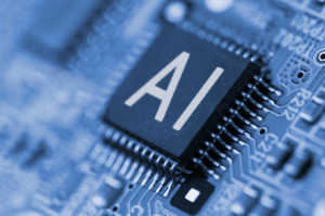
How fast can we make AI learn while using minimal energy? In the relentless pursuit of speed and energy efficiency, researchers have unveiled a novel approach to AI computation: harnessing the power of light. Scientists at MIT and others have developed a photonic processor capable of performing the essential computations of deep neural networks entirely on a chip. This breakthrough could pave the way for ultrafast, energy-efficient processors capable of real-time learning, offering an innovative alternative to traditional electronic computing hardware.
Why Photonics?
The deep neural networks that power today’s AI models rely heavily on complex linear algebra operations, such as matrix multiplication, as well as nonlinear functions that enable intricate pattern recognition. However, the ever-increasing size and complexity of these models are pushing the limits of electronic computing. Photonic hardware, which uses light instead of electricity, offers a faster and more energy-efficient solution.
Photonic systems have long promised high-speed computation, but they were hindered by their inability to perform nonlinear operations on-chip. They often require off-chip electronics that compromise their efficiency. This limitation is now overcome, thanks to a fully integrated photonic processor demonstrated by the research team.
A Decade of Innovation: Machine Learning with Light
In 2017, Englund’s group, along with the other scientists in the lab of Marin Soljačić, the Cecil and Ida Green Professor of Physics, demonstrated an optical neural network on a single photonic chip that could perform matrix multiplication with light.

Building on years of research, the team developed an optical deep neural network composed of interconnected modules that can carry out both linear and nonlinear operations. At the core of this system is the use of nonlinear optical function units (NOFUs). These innovative devices combine electronics and optics to implement nonlinear functions directly on the chip, circumventing the power-intensive nature of traditional optical nonlinearities.
The result is an optical system that maintains data in the optical domain from start to finish, achieving ultra-low latency. This allows the photonic chip to perform key computations in less than half a nanosecond, all while consuming significantly less energy than its digital counterparts.
Real-Time Learning on Photonic Chip
One of the most exciting capabilities of this photonic processor is its ability to perform in situ training — training a deep neural network directly on the chip. Traditional digital systems consume vast amounts of energy during training, making this feature particularly attractive for applications demanding real-time learning, such as navigation, telecommunications, and scientific research.
During tests, the chip achieved over 96% accuracy during training and more than 92% accuracy during inference, a performance level comparable to traditional hardware. As Saumil Bandyopadhyay, the lead author of the study, explains: “There are a lot of cases where how well the model performs isn’t the only thing that matters, but also how fast you can get an answer. Now that we have an end-to-end system that can run a neural network in optics, at a nanosecond time scale, we can start thinking at a higher level about applications and algorithms.”
The Road Ahead
This research appears in the latest issue of Nature Photonics and was led by a team of scientists including Saumil Bandyopadhyay, Alexander Sludds, Nicholas Harris, Darius Bunandar, Stefan Krastanov, Ryan Hamerly, Matthew Streshinsky, Michael Hochberg, and Dirk Englund. Collaborators span institutions like MIT, NTT Research, and the University of Massachusetts at Amherst, highlighting the collaborative spirit driving this technological leap forward.
Fabricated using standard commercial foundry processes, the photonic chip can be scaled up using existing CMOS infrastructure, making it feasible for mass production. This opens doors for integration with real-world devices, including cameras, telecommunications systems, and even lidar technologies for autonomous vehicles.
The research team is now focused on scaling the device and developing algorithms tailored to leverage the unique advantages of optical computing. “This work demonstrates that computing… can be compiled onto new architectures of linear and nonlinear physics that enable a fundamentally different scaling law of computation versus effort needed,” says Dirk Englund, senior author of the research paper and a professor in MIT’s Department of Electrical Engineering and Computer Science.
Applications Beyond Imagination
The potential applications of this technology are vast. From high-speed telecommunications to complex scientific research in particle physics and astronomy, the photonic processor could transform industries reliant on computationally demanding tasks. Its unparalleled speed and energy efficiency also make it an ideal candidate for AI applications where real-time responses are critical.
As Bandyopadhyay emphasizes, “This is especially useful for systems where you are doing in-domain processing of optical signals, like navigation or telecommunications, but also in systems that you want to learn in real-time.”
A Paradigm Shift in AI Hardware
The development of this fully integrated photonic processor marks a significant step forward in rethinking the hardware that underpins artificial intelligence. By combining the speed of light with the scalability of traditional chip fabrication, this innovation challenges the status quo, hinting at a future where light, not electricity, powers the AI revolution.